제품 상세 사양
Product Description
핵심 이점
- Uniform Microporous Structure
Uniform pore distribution ensures balanced vacuum adsorption, preventing wafer warpage or slippage during high-speed processing.
- Superior Wear & Corrosion Resistance
Resists mechanical abrasion and chemical corrosion from semiconductor process fluids, extending service life and reducing maintenance costs.
- High-Precision Dimensional Accuracy
Ultra-flat surface and tight tolerance control guarantee seamless compatibility with semiconductor wafers and chips of various specifications.
- Cleanroom Compatibility
Non-contaminating, non-outgassing material properties meet ISO Class 5 cleanroom standards, avoiding particle pollution in semiconductor manufacturing.
Typical Technical Parameters
| 매개변수 | Specification |
|---|---|
| 재료 | 99.5%+ High-Purity Alumina (Al₂O₃) |
| Pore Size | 0.5–5 μm (customizable) |
| 다공성 | 20–40% (adjustable) |
| Surface Flatness | ≤0.005 mm |
| 경도 | HRA 88–92; Mohs Hardness 9.0 |
| Max Service Temperature | 1200°C |
| Chemical Stability | Resistant to acids, alkalis, plasmas, and semiconductor process chemicals |
| Customizable Sizes | Diameter: 50–500 mm; Thickness: 10–50 mm |
애플리케이션
- Semiconductor wafer handling, dicing, lithography, and etching processes
- Silicon chip packaging and testing equipment
- Flat panel display (FPD) substrate processing
- Optical component manufacturing and precision positioning
고급 세라믹
고급 세라믹 제품군은 각기 다른 특성을 지닌 다양한 소재를 포함하며, 각 소재는 특정 애플리케이션 시나리오에 맞게 특별히 설계되었습니다.
세라믹 소재
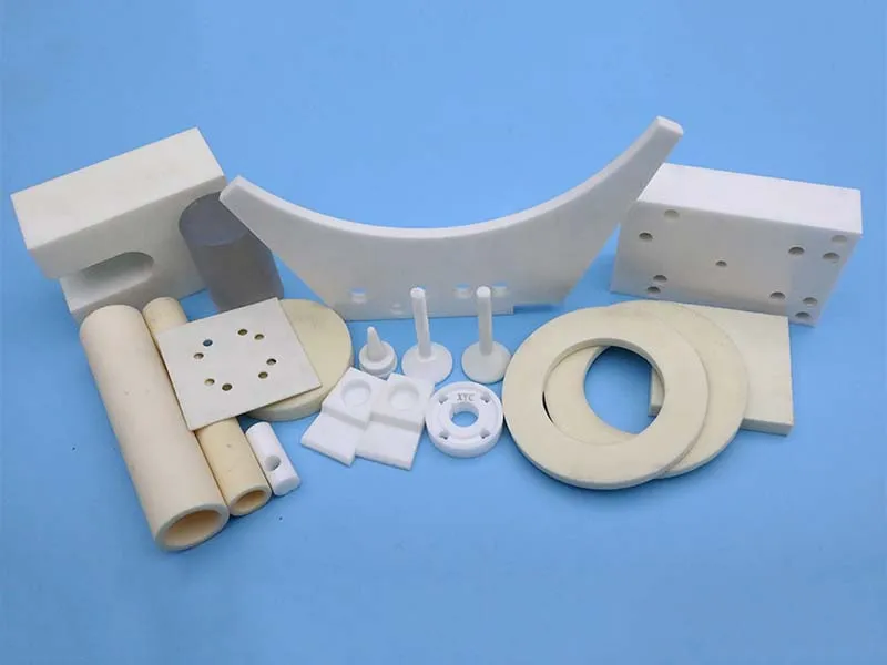
주요 적용 분야
여러 하이엔드 제조 분야에서 널리 사용되어 고객에게 맞춤형 솔루션을 제공합니다.


관련 제품 추천
다음 제품에도 관심이 있을 수 있습니다.

Silicon Nitride Ceramic Heating Plate | Ceramic Components for Molding Presses
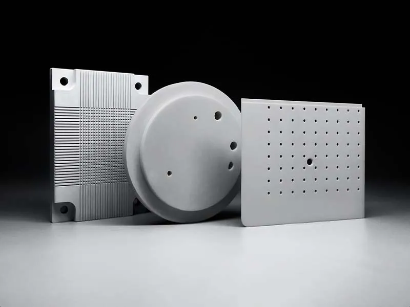
Silicon nitride (Si₃N₄) ceramic heating plates are high-performance structural ceramic components specifically engineered for demanding applications in hot pressing and molding equipment—such as those used in powder metallurgy, technical ceramics, and composite material manufacturing. Leveraging the exceptional properties of silicon nitride, these heating plates deliver outstanding mechanical strength, thermal stability, and electrical insulation even under extreme operating conditions, making them a superior alternative to conventional metal or alumina-based heating elements.
세부 정보 보기
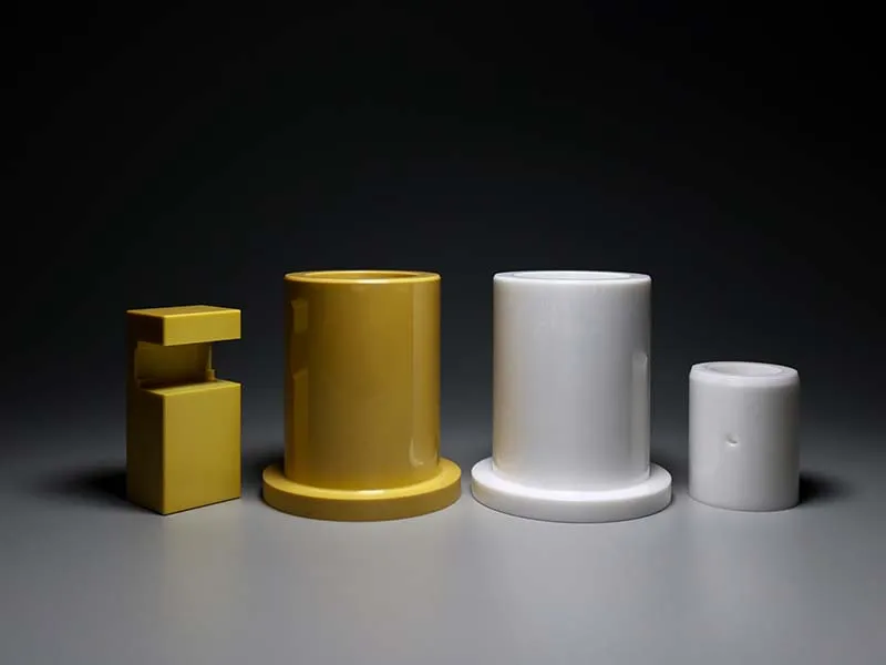
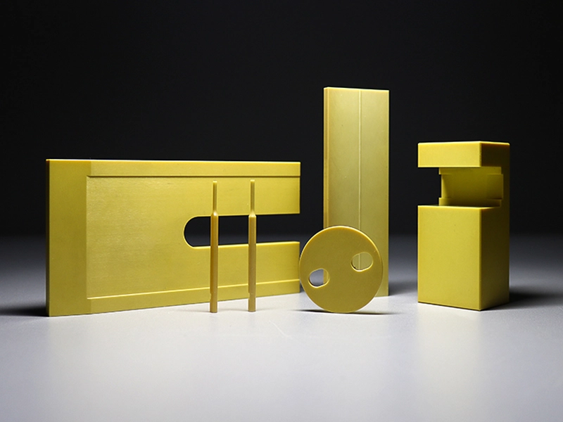
Alumina Ceramic Microporous Chuck | Semiconductor Wafer & Chip | Vacuum Chuck | Wear-Resistant Porous Ceramic
Product Description Alumina Ceramic Microporous Chuck | Semiconductor Wafer & Chip | Vacuum Chuck | Wear-Resistant Porous Ceramic Crafted from...
세부 정보 보기
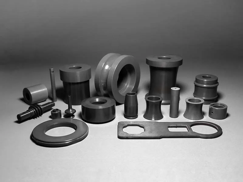
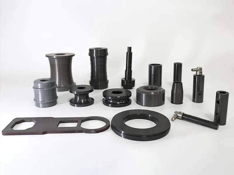
Ceramic mechanical arm / Semiconductor wafer equipment / Handling arm
Ceramic mechanical arm / Semiconductor wafer equipment / Handling arm Excellent wear resistance, high temperature resistance, corrosion resistance, thermal shock resistance,insulation and other characteristics Good price compared with traditional materials, Having strength and fracture toughness that other materials cannot achieve,suitable for highly corrosive and high-strength environments. Green and environmentally friendly
세부 정보 보기
문의 보내기
문의하기
왜 동관 XYC 신소재 유한공사 Is Your Premier Partner for Advanced Ceramics & Tungsten Carbides
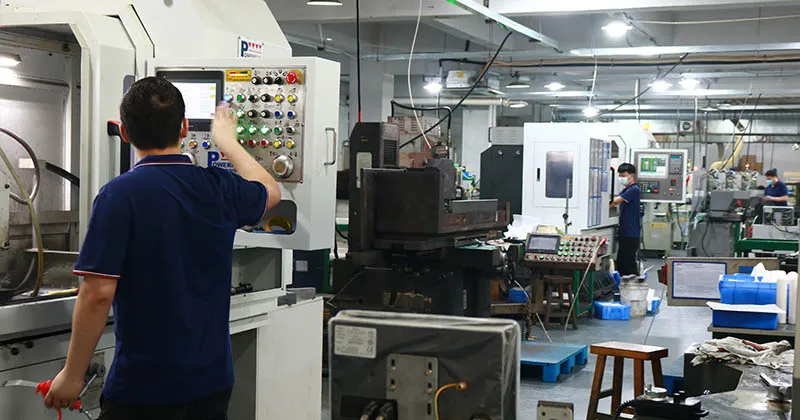
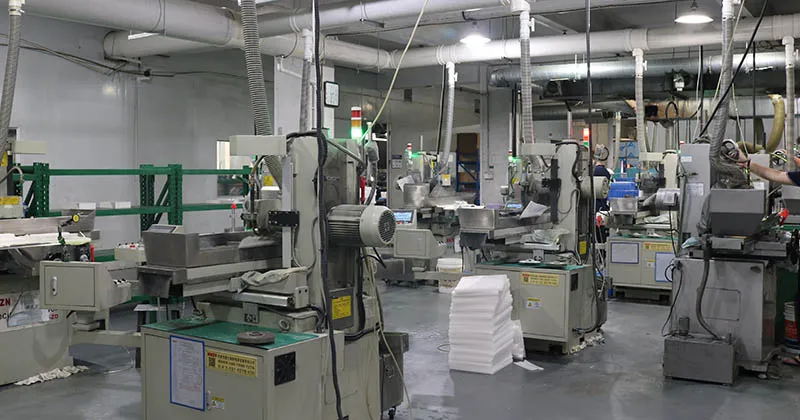
Founded in 2009, we are a leading manufacturer of advanced ceramics and tungsten carbide. We deliver precision components to 1,000+ global customers in semiconductor, automotive, medical, and energy sectors.
핵심 이점
Diverse Materials & Products
Alumina, Zirconia, Silicon Nitride, Silicon Carbide, Aluminum Nitride, and high-performance tungsten carbide; 10,000+ custom component forms, 8 million+ precision components annual output.
Ultra-High Precision & Durability
±0.001 mm machining accuracy; Ceramics resist 1800°C heat and corrosion; Tungsten steel delivers superior wear resistance.
Tailored Cross-Industry Solutions
End-to-end support from material selection to mass production, available for both small-batch prototyping and large-scale orders.