Semiconductor Ceramic Product Cases
Explore our other high-performance ceramic products developed for the semiconductor industry to meet the needs of different application scenarios

Aluminum Nitride (AlN) Ceramic Precision Structural Components | High-Thermal-Conductivity Insulating Parts for Electronic & Semiconductor Equipment (Precision Equipment Industry)
This series of high-purity aluminum nitride (AlN) ceramic structural components...
Learn More
Alumina Ceramic Microporous Vacuum Chuck | Semiconductor Wafer & Chip Handling Component | Semiconductor Industry
This high-performance alumina ceramic microporous vacuum chuck is engineered for...
Learn More
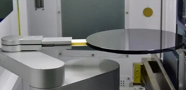
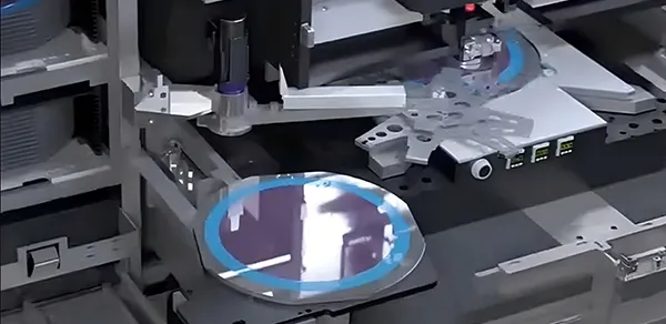
Alumina Ceramic Wafer Chuck & Handling Arm | Precision Semiconductor Manufacturing Component | Semiconductor Industry
This high-precision alumina ceramic wafer chuck and handling arm is...
Learn MoreCase Background and Challenges
With the continuous advancement of semiconductor manufacturing processes, the requirements for precision, stability, and reliability of production equipment are becoming increasingly high. Our client is a leading global semiconductor equipment manufacturer facing a series of issues caused by using traditional metal components in extreme environments (high temperature, high corrosion, high precision).
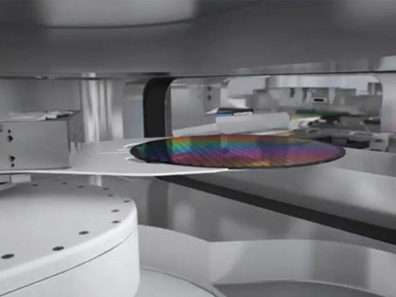
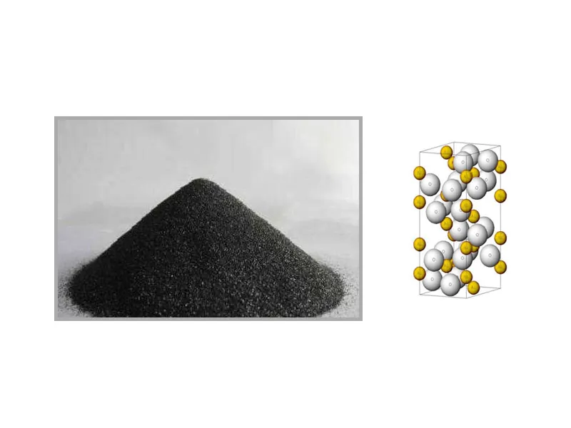
Semiconductor devices have very strict requirements for wafers. Only nearly perfect wafers can avoid electrically and mechanically harmful defects to the devices, so wafers need to go through multiple steps such as shaping, slicing, grinding, and cleaning. In these processes, wafers need a worktable for placement and fixation. Ceramic vacuum chucks, which are ceramics with a large number of interconnected or closed uniform solid or vacuum structures generated through high-temperature sintering, are used to fix workpieces such as semiconductor wafers and glass substrates through vacuum suction.
- Insufficient thermal stability in high-temperature environments leads to decreased equipment precision
- Chemical corrosion leads to short component lifespan, increasing maintenance costs and downtime
- Metal particle contamination affects semiconductor yield
- Component precision requirements reach sub-micron level
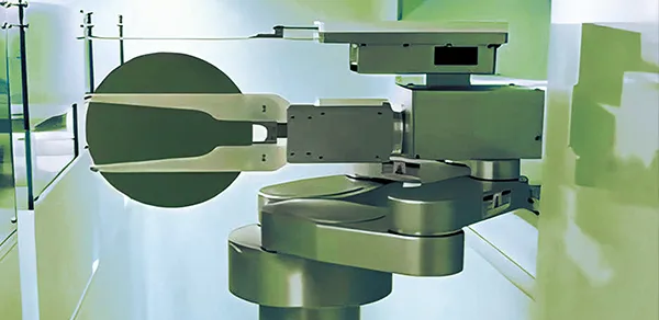
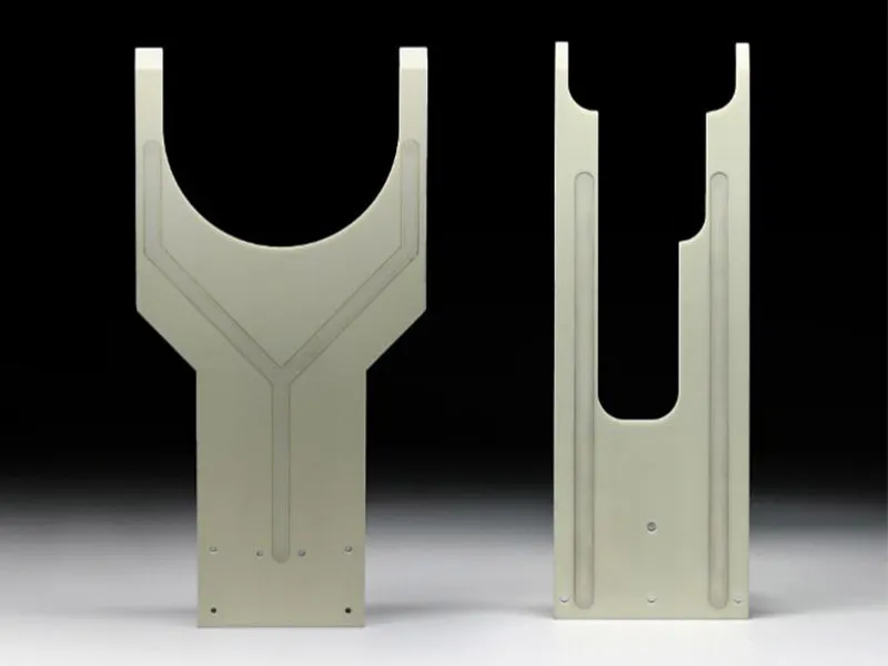
Wafer Handling Finger
Product Features/PRODUCT FEATURES
-
▲
High Airtightness
High airtightness
-
▲
Corrosion, Wear, and High Temperature Resistant
Resistant to corrosion, wear, and high temperatures
-
▲
Insulation/Anti-static
Insulation/anti-static
-
▲
High Machining Precision
High machining precision
Customized Ceramic Solutions
Based on customer needs, we have developed a series of high-precision ceramic components, using advanced material formulas and precision processing techniques, to provide ideal solutions for semiconductor manufacturing
High-temperature Ceramic Wafer Carrier
Using silicon nitride-based ceramic material, it maintains stable dimensions in 1200°C high-temperature environments, with extremely low thermal expansion coefficient, effectively preventing wafer deformation and improving yield.
Corrosion-resistant Ceramic Reaction Chamber Components
Using high-purity alumina and zirconia composite materials, it has excellent chemical inertness, effectively resisting plasma corrosion, and extending service life by more than 3 times.
High-precision Ceramic Positioning Components
Through precision grinding and polishing processes, it achieves ±0.5μm dimensional accuracy and Ra<10nm surface roughness, meeting the positioning requirements of advanced processes.
Semiconductor Manufacturing Process and Ceramic Applications
We provide professional ceramic solutions for key process links in semiconductor manufacturing, ensuring the stability and reliability of each process
| Manufacturing Process | Equipment Using Ceramic Products | Advanced Ceramic Material Components | Main Material Types |
|---|---|---|---|
| Lithography | Lithography Machine | Ceramic worktable, guide rail, mirror, ceramic chuck, arm, water-cooled plate, chuck | Alumina, Silicon Nitride, Silicon Carbide |
| Etching | Etching Machine | Ring cylinder type, gas guide type, load-bearing fixed type, gripper gasket type, guide rail, module | Zirconia, Alumina, Silicon Carbide |
| Thin Film Deposition | PVD, CVD and ALD Equipment | Ring cylinder type, gas guide type, load-bearing fixed type, gripper gasket type, module | Zirconia, Alumina, Silicon Carbide |
| Ion Implantation | Ion Implantation Equipment | Ring cylinder type, load-bearing fixed type, gripper gasket type | Zirconia, Alumina, Silicon Carbide |
| Coating and Development | Lithography Machine, Coating and Development Equipment | Load-bearing fixed type, gripper gasket type | Alumina, Silicon Carbide |
| Oxidation/Diffusion, Annealing, Alloying, etc. | Oxidation and Diffusion Equipment | Load-bearing fixed type, gripper gasket type, module | Alumina |
Ceramic Component Applications in Key Equipment
Lithography Machine
Core ceramic components: Precision positioning worktable, mirror system, vacuum chuck, requiring extremely high flatness and thermal stability.
Etching Machine
Core ceramic components: Reaction chamber inner wall, gas distributor, electrode base, requiring excellent corrosion resistance and high-temperature stability.
Thin Film Deposition Equipment
Core ceramic components: Crucible, evaporation source, gas nozzle, requiring high purity, low volatility and excellent thermal cycle stability.
Rigorous Project Implementation Process
From requirement analysis to final delivery, we follow a strict quality management system to ensure each ceramic component meets the customer's high standards
Requirement Analysis and Material Selection
Our engineering team communicates deeply with customers, analyzes usage environments and technical requirements, selects the most suitable ceramic material combination, and conducts preliminary performance evaluation and simulation tests.
Precision Mold Design and Manufacturing
Based on 3D modeling and finite element analysis, we design high-precision molds and use CNC machining technology to ensure mold precision, laying the foundation for subsequent forming processes.
Forming and Sintering Process
We use isostatic pressing technology to ensure uniform green body density and conduct high-temperature sintering in a strictly controlled atmosphere furnace to ensure the material achieves optimal performance.
Precision Machining and Surface Treatment
Using advanced CNC machining centers and ultra-precision grinding equipment, combined with proprietary processes, we achieve sub-micron precision machining to ensure surface quality meets requirements.
Strict Quality Inspection
We conduct comprehensive inspections through advanced equipment such as coordinate measuring machines, laser interferometers, and scanning electron microscopes to ensure each component meets technical specifications.
Project Results and Customer Benefits
Customer Feedback
XYC Ceramics' high-precision ceramic components have completely solved the material corrosion and precision instability issues we faced in semiconductor manufacturing. The equipment maintenance frequency has been significantly reduced, and both production efficiency and product yield have been greatly improved. We are deeply impressed by their professional technical support and customized services.
Engineer Zhang
R&D Director | A Semiconductor Equipment Manufacturer
Semiconductor-specific Ceramic Core Products
We provide high-precision, high-performance ceramic core components for semiconductor manufacturing to ensure the stability and reliability of the production process
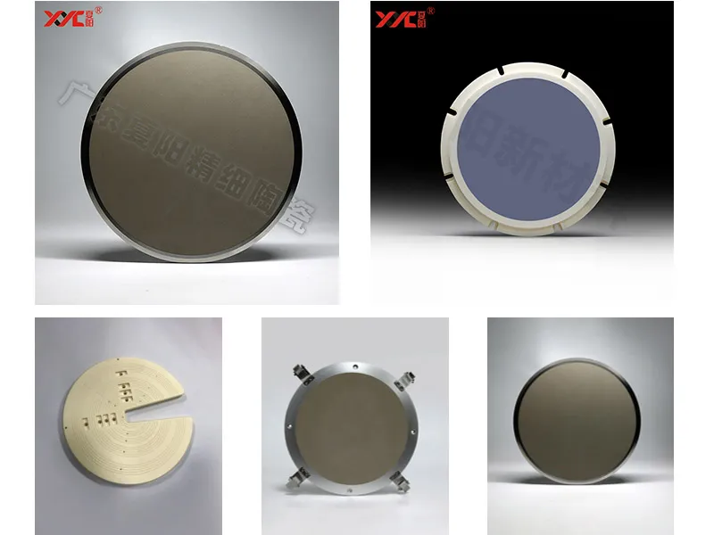
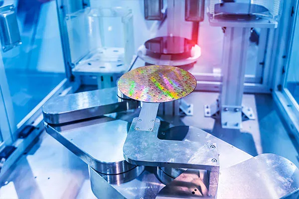
Ceramic Vacuum Chuck
Ceramic vacuum chuck is a special vacuum chuck made of porous ceramic materials, with high porosity, high strength, high flatness and other characteristics, widely used in semiconductor wafer cutting, grinding, inspection and other processes.
Core Performance Features:
- Self-sealing Test:Turn off the vacuum source, negative pressure from -85Kpa to -80Kpa, duration up to 60s or more
- Wafer Adsorption Test:Turn off the vacuum source, negative pressure from -80Kpa to -25Kpa, duration up to 35s or more
- High Precision:Excellent flatness and parallelism, meeting sub-micron level positioning requirements
- Good Air Tightness:Uniform pore distribution, ensuring stable vacuum adsorption effect
- Good High Temperature Resistance:Can work stably in high temperature environments, no deformation, no aging
- Controllable Surface Resistivity:Effectively prevents static accumulation, protects sensitive wafer surfaces
Semiconductor Equipment Ceramic Components
The advanced ceramic material components used by the company in semiconductor equipment are mainly applied inside the chamber, and some of them are in direct contact with wafers, which are key precision components in integrated circuit manufacturing.
Application Features:
- High-purity materials, no metal ion contamination, ensuring a clean wafer manufacturing environment
- Excellent chemical corrosion resistance, resisting various process gases and plasma erosion
- Extremely low particle shedding rate, meeting ultra-clean room environment requirements
- Precise dimensional control, meeting sub-micron assembly tolerance requirements
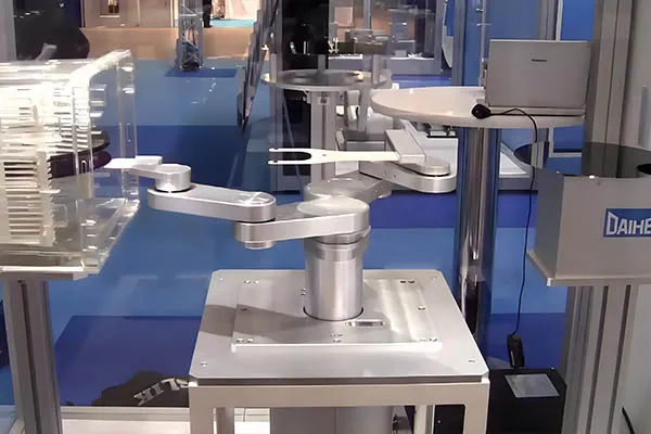
Ceramic Robotic Arm
Used for transferring wafers and LEDs throughout the production process, effectively preventing wafer scratches and surface contamination. Ceramic robotic arms are made of advanced ceramic materials, featuring excellent rigidity, lightweight characteristics, and chemical stability.
Key Advantages:
Advanced Precision Manufacturing
XYC has over 20 years of precision processing experience!
We are equipped with a large number of processing equipment, covering various high-precision processing equipment at home and abroad, capable of handling the processing of various complex workpieces.
Raw Material Preparation
RAW MATERIAL PREPARATION
XYC has its own material R&D production line and can conduct production and sintering according to different materials and sizes!
XYC has its own material R&D production line and can conduct production and sintering according to different materials and sizes!
Precision Inspection
PRECISION INSPECTION
XYC has IQC, IPQC, and OQC departments, and owns multiple imported high-precision inspection equipment, which can meet various industry standard inspection requirements, such as Zeiss coordinate measuring machine, CCD, SEM, etc.
XYC Advantages
R&D Strength
The company has an R&D team led by well-known professors and doctors in the ceramic materials industry, with more than 30 professional and technical personnel, and also receives strong R&D support from research institutes and university-enterprise cooperation.
Powder Formula
With multiple material doctors and rich application case experience, we can develop formulas according to customer needs to meet customer requirements.
Forming and Sintering
We have various forming and sintering equipment, which can perform corresponding forming and sintering according to different material requirements.
Precision Processing Strength
With more than 20 years of precision processing experience, we have complete processing equipment for each process and can customize solutions according to customer requirements in depth.
High Quality Assurance
The company has IQC, IPQC, and OQC departments, and owns multiple high-precision testing equipment to strictly control quality, which can meet various industry standard testing requirements.
Complete Industrial Chain
The company has a complete closed-loop industrial chain, from formula → forming → sintering → precision manufacturing → high-clean cold surface treatment → solution testing, all completed by our company.
Need Semiconductor Ceramic Solutions?
Whatever challenges you face, we can provide you with customized ceramic solutions. Contact us immediately to start cooperation!
Consult Custom Solutions