Semiconductor Equipment – Ceramic Vacuum Chuck
Ceramic vacuum chucks are a special type of vacuum pad made from porous ceramic materials, featuring high porosity, high strength, and excellent surface flatness. They are widely used in semiconductor wafer processes such as slicing, grinding, polishing, and inspection.
Product Features
- High precision
- Excellent air tightness
- Uniform suction force
- Wear-resistant and corrosion-resistant
▲ Surface flatness can reach 0.002 mm; parallelism can reach 0.003 mm
表格
| Material | Pore Size (μm) | Porosity | Pressure Differential (bar) | Resistivity | Color |
|---|---|---|---|---|---|
| Aluminum Oxide | 5–50 | 15–45% | 35 | 1×10¹¹ Ω·cm | Dark gray / Earth yellow |
| Silicon Carbide | 10–50 | 15–45% | 30 | 1×10⁸ Ω·cm | Black |

Product Features – Ceramic Robotic Arms for Semiconductor Equipment
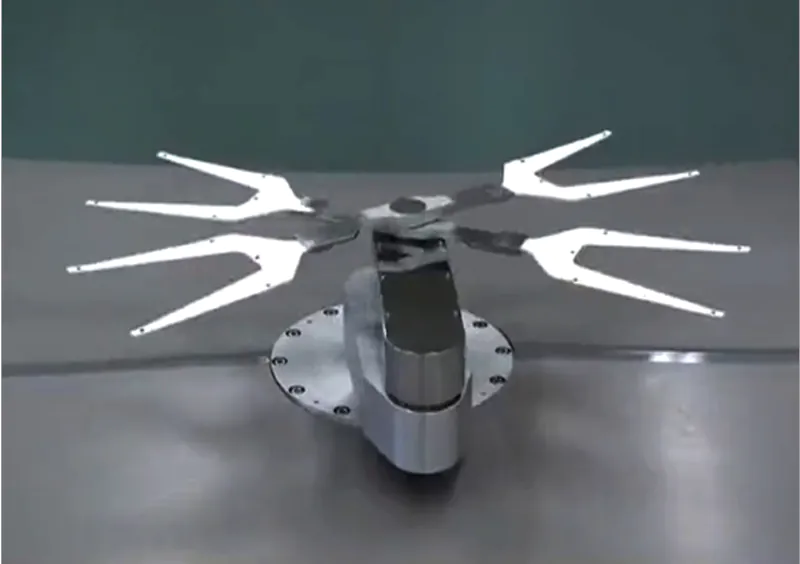
wafer handling finger
Ceramic mechanical arms, also known as ceramic robotic fingers, wafer carriers, or ceramic handling arms, are primarily used in semiconductor equipment for transporting and transferring wafers. They function as the “hands” of semiconductor equipment robots, responsible for precisely moving circular silicon wafers to designated positions.
Product Features
- High product precision
- Excellent air tightness
- Good high-temperature resistance
- Controllable surface resistivity
- Strong resistance to acids, alkalis, and corrosion, suitable for extremely harsh environments
▲ Self-sealing test: Turn off the vacuum air source; maintain a negative pressure from –85 kPa to –80 kPa for more than 60 seconds.
▲ Wafer adsorption test: Turn off the vacuum air source; maintain a negative pressure from –80 kPa to –25 kPa for more than 35 seconds.
- High Dimensional Precision: Ensures accurate wafer handling and positioning critical for advanced semiconductor processes.
- Exceptional Air Tightness: Maintains stable vacuum conditions during wafer transfer, minimizing contamination risks.
- Superior High-Temperature Resistance: Suitable for high-temperature process environments without deformation or performance degradation.
- Controllable Surface Resistivity: Engineered resistivity enables electrostatic control and prevents charge buildup, protecting sensitive wafers.
- Outstanding Chemical Resistance: Highly resistant to strong acids, alkalis, and corrosive process gases—ideal for harsh semiconductor fabrication environments.
Performance Validation Tests
▲ Self-Sealing Test: With the vacuum source turned off, the arm maintains a negative pressure of –85 kPa to –80 kPa for over 60 seconds.
▲ Wafer Holding Test: With the vacuum source turned off, it sustains a negative pressure of –80 kPa to –25 kPa for more than 35 seconds, ensuring reliable wafer retention.
Key Performance Specifications
| Parameter | Unit | Silicon Carbide (SiC) | Aluminum Oxide (Al₂O₃) |
|---|---|---|---|
| Surface Resistivity | Ω | 1 × 10⁵ | 1 × 10¹⁴ |
| Max. Operating Temp. (Split Arm) | °C | 350 | 350 |
| Max. Operating Temp. (Integrated Arm) | °C | 800 | 800 |
| Adsorption Surface Roughness (Ra) | μm | 0.01 | 0.01 |
| Adsorption Surface Flatness | mm | 0.01 | 0.01 |
Note: All values reflect typical performance under standard cleanroom and process conditions.


